- 您现在的位置:买卖IC网 > Sheet目录3862 > PIC16F916-I/ML (Microchip Technology)IC PIC MCU FLASH 8KX14 28QFN
207
8018P–AVR–08/10
ATmega169P
20.4
USI Register Descriptions
20.4.1
USIDR – USI Data Register
The USI uses no buffering of the Serial Register, that is, when accessing the Data Register
(USIDR) the Serial Register is accessed directly. If a serial clock occurs at the same cycle the
register is written, the register will contain the value written and no shift is performed. A (left) shift
operation is performed depending of the USICS1..0 bits setting. The shift operation can be con-
trolled by an external clock edge, by a Timer/Counter0 Compare Match, or directly by software
using the USICLK strobe bit. Note that even when no wire mode is selected (USIWM1..0 = 0)
both the external data input (DI/SDA) and the external clock input (USCK/SCL) can still be used
by the Shift Register.
The output pin in use, DO or SDA depending on the wire mode, is connected via the output latch
to the most significant bit (bit 7) of the Data Register. The output latch is open (transparent) dur-
ing the first half of a serial clock cycle when an external clock source is selected (USICS1 = 1),
and constantly open when an internal clock source is used (USICS1 = 0). The output will be
changed immediately when a new MSB written as long as the latch is open. The latch ensures
that data input is sampled and data output is changed on opposite clock edges.
Note that the corresponding Data Direction Register to the pin must be set to one for enabling
data output from the Shift Register.
20.4.2
USISR – USI Status Register
The Status Register contains Interrupt Flags, line Status Flags and the counter value.
Bit 7 – USISIF: Start Condition Interrupt Flag
When Two-wire mode is selected, the USISIF Flag is set (to one) when a start condition is
detected. When output disable mode or Three-wire mode is selected and (USICSx = 0b11 &
USICLK = 0) or (USICS = 0b10 & USICLK = 0), any edge on the SCK pin sets the flag.
An interrupt will be generated when the flag is set while the USISIE bit in USICR and the Global
Interrupt Enable Flag are set. The flag will only be cleared by writing a logical one to the USISIF
bit. Clearing this bit will release the start detection hold of USCL in Two-wire mode.
A start condition interrupt will wakeup the processor from all sleep modes.
Bit 6 – USIOIF: Counter Overflow Interrupt Flag
This flag is set (one) when the 4-bit counter overflows (that is, at the transition from 15 to 0). An
interrupt will be generated when the flag is set while the USIOIE bit in USICR and the Global
Interrupt Enable Flag are set. The flag will only be cleared if a one is written to the USIOIF bit.
Clearing this bit will release the counter overflow hold of SCL in Two-wire mode.
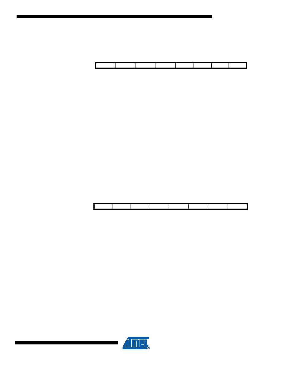
Bit
7
6
5
4
3
2
1
0
(0xBA)
MSB
LSB
USIDR
Read/Write
R/W
Initial Value
0
Bit
7
6
5
4
3
210
(0xB9)
USISIF
USIOIF
USIPF
USIDC
USICNT3
USICNT2
USICNT1
USICNT0
USISR
Read/Write
R/W
R
R/W
Initial Value
0
发布紧急采购,3分钟左右您将得到回复。
相关PDF资料
PIC16C716-20I/P
IC MCU OTP 2KX14 A/D PWM 18DIP
PIC18F26K80-I/SO
MCU PIC 64KB FLASH 28SOIC
PIC18F26J13-I/SS
IC PIC MCU 64KB FLASH 28SSOP
SFW27R-1STE1
SFW27R-1STE1-FFC/FPC CONN
PIC18F66J15-I/PT
IC PIC MCU FLASH 48KX16 64TQFP
PIC24FV32KA302-I/SO
MCU 32KB FLASH 2KB RAM 28-SOIC
PIC24HJ64GP204-I/ML
IC PIC MCU FLASH 64K 44-QFN
SFW27R-2STE1
SFW27R-2STE1-FFC/FPC CONN
相关代理商/技术参数
PIC16F916-I/SO
功能描述:8位微控制器 -MCU 14KB FL 352R 25 I/O RoHS:否 制造商:Silicon Labs 核心:8051 处理器系列:C8051F39x 数据总线宽度:8 bit 最大时钟频率:50 MHz 程序存储器大小:16 KB 数据 RAM 大小:1 KB 片上 ADC:Yes 工作电源电压:1.8 V to 3.6 V 工作温度范围:- 40 C to + 105 C 封装 / 箱体:QFN-20 安装风格:SMD/SMT
PIC16F916-I/SO
制造商:Microchip Technology Inc 功能描述:8 Bit Microcontroller Clock Speed:20MHz
PIC16F916-I/SOG
制造商:Microchip Technology Inc 功能描述:8BIT MCU FLASH SMD 16F916 SOIC28
PIC16F916-I/SP
功能描述:8位微控制器 -MCU 14KB FL 352R 25 I/O RoHS:否 制造商:Silicon Labs 核心:8051 处理器系列:C8051F39x 数据总线宽度:8 bit 最大时钟频率:50 MHz 程序存储器大小:16 KB 数据 RAM 大小:1 KB 片上 ADC:Yes 工作电源电压:1.8 V to 3.6 V 工作温度范围:- 40 C to + 105 C 封装 / 箱体:QFN-20 安装风格:SMD/SMT
PIC16F916-I/SP
制造商:Microchip Technology Inc 功能描述:8 Bit Microcontroller Clock Speed:20MHz
PIC16F916-I/SS
功能描述:8位微控制器 -MCU 14KB FL 352R 25 I/O RoHS:否 制造商:Silicon Labs 核心:8051 处理器系列:C8051F39x 数据总线宽度:8 bit 最大时钟频率:50 MHz 程序存储器大小:16 KB 数据 RAM 大小:1 KB 片上 ADC:Yes 工作电源电压:1.8 V to 3.6 V 工作温度范围:- 40 C to + 105 C 封装 / 箱体:QFN-20 安装风格:SMD/SMT
PIC16F916-I/SS
制造商:Microchip Technology Inc 功能描述:8-Bit Microcontroller IC
PIC16F916T-E/MLC02
制造商:Microchip Technology Inc 功能描述: